1.
Key features
of the RT6190
Programmable functionalities via I2C control
The RT6190 can operate with a wide input voltage range of 4.5V to 36V, and the output voltage can be programmed between 3V and 36V. This controller is designed with an I2C compatible interface, which supports many programmable functions, such as CV/CC output, switching frequency (250kHz to 1MHz), and cable voltage drop compensation during long-distance transmission.
USB-PD 3.0 SPR and 3.1 EPR support
The RT6190 implements peak current mode control mechanism with the programmable constant voltage in 12.5mV/step (typ.) and constant current in 9-Bit Resolution output to support USB-PD 3.0 SPR mode and 28V of 3.1 EPR mode.
Great control of power stage with both MOSFETs and GaN FETs
It has built-in charge pumps for driving external low-cost N-MOSFETs and GaN FETs, which are currently gaining popularity in the market.
Broad range of applications
The RT6190 can control USB ports (1A + 1C), making it ideal for applications with USB ports at power supply or system side. However, it does not include the functionality to control USB-C CC line, which can be completed by the main controller or an external TCPC controller such as RT1718S.
2.
Design
Examples
Typical application circuit for forward and reverse operation
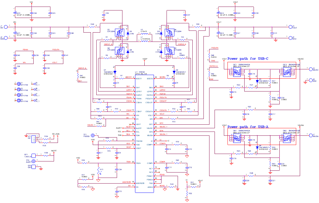
The RT6190 datasheet provides several application circuits for different scenarios. The most common bi-directional buck-boost circuit is shown in the diagram 1. The core functionality of the RT6190 is to control the operation of switches shown in the diagram, including Q1, Q2, Q3, and Q4, which can be selected based on specific application requirements.
An external controller communicates with the RT6190 through the I2C interface, and the control commands are written into its registers to execute. As it can be seen at Note (2) which is a simple demonstration of a forward conversion: First, the external power supply is connected to VSYS, and EN is also connected to enable the device. Then, the control instructions 90h and 02h are written into the registers at internal registers 0x0E and 0x29, respectively (0x0E = 90h, 0x29 = 02h). The function of 0x0E = 90h is to enable EN_PWM = 1 to start the buck-boost conversion, and the function of 0x29 = 02h is to turn on the blocking switch QC1/2. Since the output voltage and output current control values have pre-set parameters, 5V will automatically appear on the USB-C port. As Note (3) indicates, it is to put the RT6190 into the reverse conversion mode where the VSYS will be 5V.

Note:
(1) I2C slave address is 0x2C when R17 = NC, R18 = 100kΩ.
I2C slave address is 0x2D when R17 = 100kΩ, R18 = NC.
(2) For Forward operation:
- Connect input power supply to VSYS and EN pin, and connect e-load to VBUSC.
- Set 0x0E = 90h, 0x29 = 02h, then VBUSC will be 5V.
(3) For Reverse operation:
- Connect input power supply to VBUSC and EN pin, and connect e-load to VSYS.
- Set 0x0C = 52h, 0x29 = 02h, 0x0E = 90h, then VSYS will be 5V.
(4) Support 1C1A when VBUS = 5V.
*: Optional components R5, R6, C1 and C2 are used for Snubber.
RT6190 + MCU (with CC Logic) for Monitors
Based on the diagram 1, we can add a MCU or an application processor to make a practical design for display applications shown as the diagram 2. The circuity looks quite simple because it does not include a USB-A port. However, the connected MCU/EC must have the CC processing logic for USB-C interface applications.

Note:
(1) I2C slave address is 0x2C when R17 = NC, R18 = 100kΩ.
I2C slave address is 0x2D when R17 = 100kΩ, R18 = NC.
(2) VBUSA and GPA can be floating if VBUSC used only.
*: Optional components R5, R6, C1 and C2 are used for Snubber.
RT6190 + TCPC IC (RT1718S) for Monitors
If the application requires USB-PD protocol support, a TCPC Type-C port controller is required. The diagram 3 shows an example where the RT1718S is added.

Note:
(1) I2C slave address is 0x2C when R17 = NC, R18 = 100kΩ.
I2C slave address is 0x2D when R17 = 100kΩ, R18 = NC.
(2) VBUSA and GPA can be floating if VBUSC used only.
(3) *: Optional components
- R5, R6, C1 and C2 are used for Snubber.
- R31 = 0Ω, R32 = NC, QC1 and QC2 controlled by RT6190.
R31 = NC, R32 = 0Ω, QC1 and QC2 controlled by RT1718S.
- Refer to RT1718S datasheet to set R33 and R34 for VDC pin.
3.
Reference
Designs
We have teamed up with EPC, the provider of gallium nitride (GaN)-based power management technology to launch a new reference design for fast charging applications, achieving high power density and up to 98% efficiency for applications, such as power banks, mobile phone chargers, car chargers, e-bikes and solar applications.
Supporting up to 140-watt fast charging, the newly released reference design uses the RT6190 and the EPC2204 100V enhancement-mode GaN FETs. This combination shrinks the total solution size by over 20% compared to traditional solutions and achieves 98% efficiency for 20V output voltage. The features of fast switching, high efficiency and small size make it an ideal solution for battery chargers, battery stabilizers at a fixed voltage and USB-PD 3.1 fast charging (supporting 5V, 20V, and 28V).